新闻资讯banner

About PCBA electrical reliability
- Categories:PCBA technical articles
- Author:SAJ
- Origin:
- Time of issue:2021-06-16
- Views:0
(Summary description)We know that a PCB circuit board usually undergoes SMT chip processing, flow soldering, wave soldering, rework and other processes. Undoubtedly, the more links you go through, the more likely it is that some residue will be attached to the board. If it is in a humid environment or under a certain voltage, an electrochemical reaction may occur with the conductor, causing a decrease in the surface insulation resistance (SIR). If the residue on the board has formed crystals, it is very likely to cause a short circuit in the wire, which will cause the risk of electromigration (commonly known as "leakage"). In order to ensure the electrical reliability of the product, it is necessary to evaluate the performance of different no-clean fluxes. It is recommended that the same PCB be used as much as possible to use the same flux or be cleaned after soldering.
In addition, through the...

About PCBA electrical reliability
(Summary description)We know that a PCB circuit board usually undergoes SMT chip processing, flow soldering, wave soldering, rework and other processes. Undoubtedly, the more links you go through, the more likely it is that some residue will be attached to the board. If it is in a humid environment or under a certain voltage, an electrochemical reaction may occur with the conductor, causing a decrease in the surface insulation resistance (SIR). If the residue on the board has formed crystals, it is very likely to cause a short circuit in the wire, which will cause the risk of electromigration (commonly known as "leakage"). In order to ensure the electrical reliability of the product, it is necessary to evaluate the performance of different no-clean fluxes. It is recommended that the same PCB be used as much as possible to use the same flux or be cleaned after soldering.
In addition, through the...
- Categories:PCBA technical articles
- Author:SAJ
- Origin:
- Time of issue:2021-06-16
- Views:0
We know that a PCB circuit board usually undergoes SMT chip processing, flow soldering, wave soldering, rework and other processes. Undoubtedly, the more links you go through, the more likely it is that some residue will be attached to the board. If it is in a humid environment or under a certain voltage, an electrochemical reaction may occur with the conductor, causing a decrease in the surface insulation resistance (SIR). If the residue on the board has formed crystals, it is very likely to cause a short circuit in the wire, which will cause the risk of electromigration (commonly known as "leakage"). In order to ensure the electrical reliability of the product, it is necessary to evaluate the performance of different no-clean fluxes. It is recommended that the same PCB be used as much as possible to use the same flux or be cleaned after soldering.
In addition, through the reliability analysis of the mechanical strength of the solder joints, tin whiskers, voids, cracks, intermetallic compounds, mechanical vibration failure, thermal cycle failure, etc., these failures are more likely to occur. On the solder joints with the following defects: 1. After welding, the thickness of the intermetallic compound is too thin or too thick; 2. There are voids and micro cracks inside or at the interface of the solder joint; 3. The wetting area of the solder joint is small (the component solder end The size of the overlap with the pad is too small); 4. The microstructure of the solder joint is not dense, the crystal particles are large, and the internal stress is large. Of course, some defects can be detected by visual inspection, AOI or X-ray, such as small overlap size of solder joints, pores on the surface of solder joints, more obvious cracks, etc.
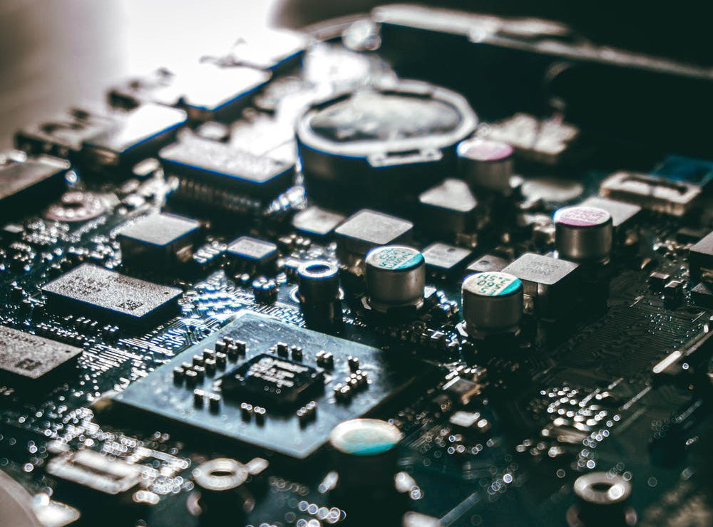
However, the microstructure of solder joints, internal stress, internal voids and cracks, especially the thickness of intermetallic compounds, these hidden defects are invisible to the naked eye. Whether it is through manual or automatic inspection of SMT processing, it cannot be detected. This requires the use of various reliability tests and analysis for detection, such as temperature cycling, vibration test, drop test, high temperature storage test, damp heat test, electromigration ( ECM) test, highly accelerated life test and highly accelerated stress screening; then conduct electrical and mechanical properties (such as solder joint shear strength, tensile strength) testing; finally pass visual inspection, X-ray fluoroscopy, metallographic section, Tests and analysis such as scanning electron microscope can make judgments.
At the same time, these hidden defects add uncertainty to the long-term reliability of lead-free products. But no matter what kind of defect, it is related to the lead-free high tin, high temperature, poor wettability, material compatibility, design, process, management and other factors. Therefore, we must consider the compatibility of lead-free materials at the beginning of the design of PCBA lead-free products; the compatibility of lead-free with design and process; at the same time, we must fully consider the heat dissipation of materials, and carefully select PCB board, The surface layer of the pad, components, solder paste and flux, etc., should be optimized accordingly to the SMT process, and more detailed process control and material management can effectively avoid or reduce product defects, thereby ensuring the electrical reliability of PCBA.
Okay, Sanjing will share it here today, I hope it can be helpful to everyone!
Scan the QR code to read on your phone


Copyright©Sanjing Electronic Technology Co., Ltd. All Rights Reserved 粤ICP备09210657号
 400-1668-717

 Feedback