新闻资讯banner

About SMT component placement on printed circuit boards
- Categories:SMT technology article
- Author:SAJ
- Origin:
- Time of issue:2021-08-28
- Views:0
(Summary description)As we all know, PCB has conductive traces, and each SMT component on the board is placed in a specific position on the conductive path. This particular component can receive enough power to play its role. If you consider using SMT (Surface Mount Technology) components to be placed on the PCB (Printed Circuit Board), special attention is needed. Let’s take a look at the following Sanjing:
When establishing SMT component placement tolerance and spacing, many factors must be considered, such as the coefficient of thermal expansion (CTE), which is one of the most important factors regarding SMT component spacing and placement. Many printed circuit boards are made of glass epoxy substrates with lead-free ceramic chip carriers. When the CTE difference between the ceramic carrier and the epoxy substrate is too large, solder joint cracks may be encountered . The solution is to ensure that the substrate has a sufficient coefficient of thermal expansion, use a compatible top substrate or...

About SMT component placement on printed circuit boards
(Summary description)As we all know, PCB has conductive traces, and each SMT component on the board is placed in a specific position on the conductive path. This particular component can receive enough power to play its role. If you consider using SMT (Surface Mount Technology) components to be placed on the PCB (Printed Circuit Board), special attention is needed. Let’s take a look at the following Sanjing:
When establishing SMT component placement tolerance and spacing, many factors must be considered, such as the coefficient of thermal expansion (CTE), which is one of the most important factors regarding SMT component spacing and placement. Many printed circuit boards are made of glass epoxy substrates with lead-free ceramic chip carriers. When the CTE difference between the ceramic carrier and the epoxy substrate is too large, solder joint cracks may be encountered . The solution is to ensure that the substrate has a sufficient coefficient of thermal expansion, use a compatible top substrate or...
- Categories:SMT technology article
- Author:SAJ
- Origin:
- Time of issue:2021-08-28
- Views:0
As we all know, PCB has conductive traces, and each SMT component on the board is placed in a specific position on the conductive path. This particular component can receive enough power to play its role. If you consider using SMT (Surface Mount Technology) components to be placed on the PCB (Printed Circuit Board), special attention is needed. Let’s take a look at the following Sanjing:
When establishing SMT component placement tolerance and spacing, many factors must be considered, such as the coefficient of thermal expansion (CTE), which is one of the most important factors regarding SMT component spacing and placement. Many printed circuit boards are made of glass epoxy substrates with lead-free ceramic chip carriers. When the CTE difference between the ceramic carrier and the epoxy substrate is too large, solder joint cracks may be encountered . The solution is to ensure that the substrate has a sufficient coefficient of thermal expansion, use a compatible top substrate or use a lead-containing ceramic chip carrier instead of a lead-free ceramic chip carrier.
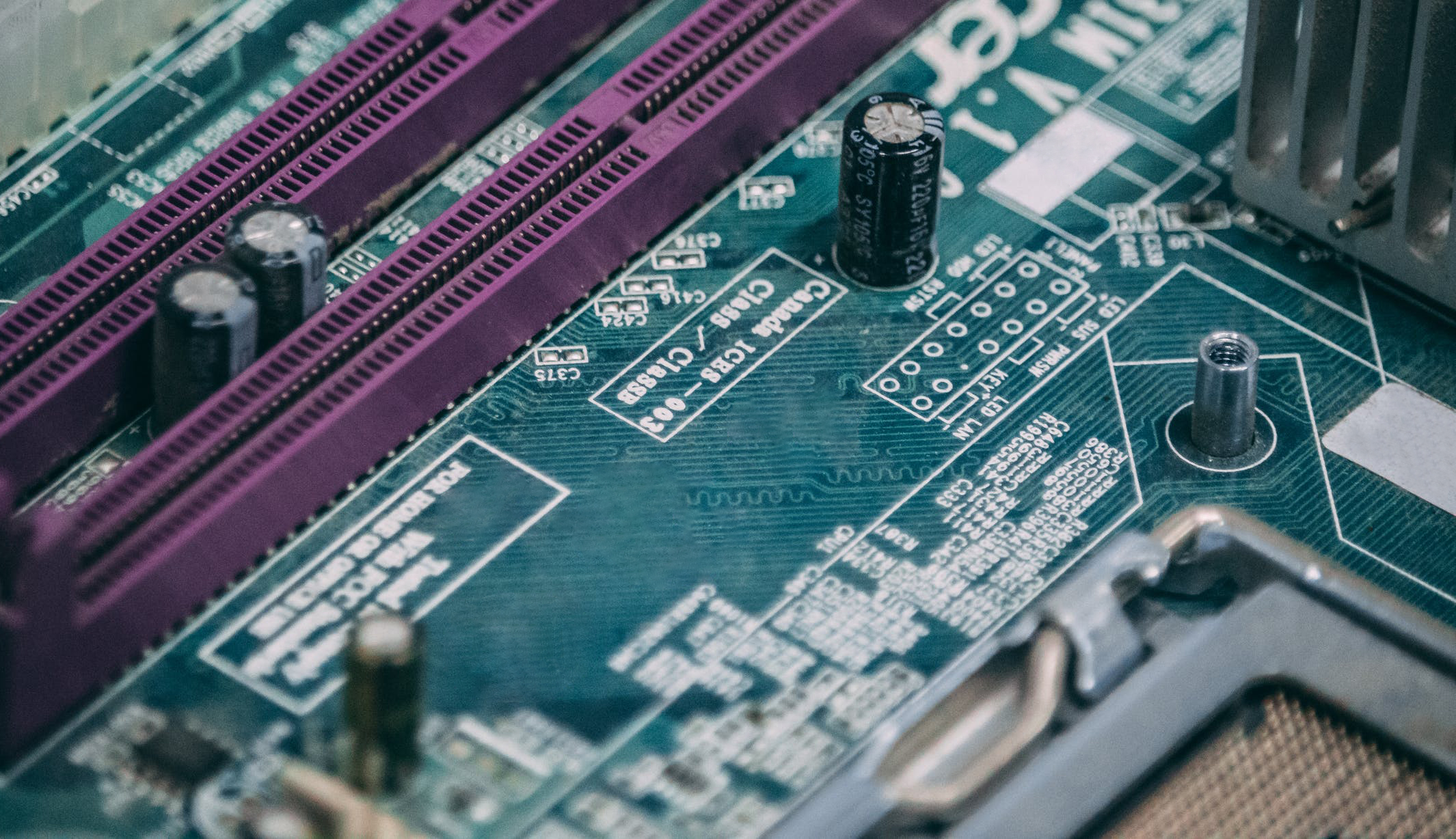
The placement of SMT components also depends on size and cost. Components that absorb more than 10mW or conduct more than 10mA require more consideration of heat and electricity. Power management components need a ground plane or power plane to control heat flow. The high-current connection depends on the acceptable voltage drop of the connection. When performing layer conversion, the high-current path requires two to four through holes at each layer transition. When multiple through holes are placed at the layer transition, the thermal conductivity will be improved, the reliability will be improved, and the resistance and inductance loss will be reduced.
When placing SMT components, first place the connectors, and then place the power circuit, sensitive and precision circuits, key circuit components, and any other necessary components. The routing priority is selected based on the power level, noise sensitivity, and generation and routing functions. The number of layers included varies according to the power level and the complexity of the design.
After placing the components, check the layout and make necessary adjustments to the physical location or wiring path. The final consideration should be to ensure that there is a solder mask between the pins and the vias, and the screen printing is simple and protects sensitive circuits and nodes from noise The impact of the source.
The above is about the placement of SMT components on the printed circuit board, I hope it can be helpful to everyone!
Scan the QR code to read on your phone


Copyright©Sanjing Electronic Technology Co., Ltd. All Rights Reserved 粤ICP备09210657号
 400-1668-717

 Feedback