新闻资讯banner

Causes of defects in PCB pads after wave soldering
- Categories:FAQ
- Author:SAJ
- Origin:
- Time of issue:2021-07-02
- Views:0
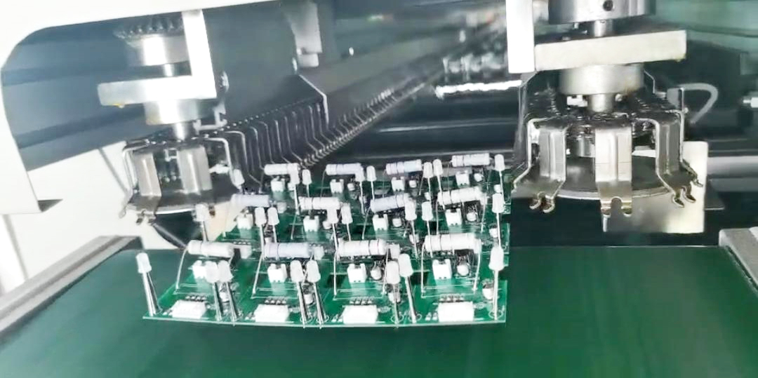
(Summary description)We know that whether it is PCBA or PCB, various defects will inevitably appear in the manufacturing process. Generally, external (visible to the naked eye) defects can be avoided with a little attention during production and processing, but internal (product itself) defects need to be paid attention to in the early stage of production and processing. Today we will mainly summarize and share the causes of defects and solutions when PCB pads undergo wave soldering. We hope to be helpful to everyone!
The more common defect problems that appear when PCB pads undergo wave soldering mainly include the following situations:
First, the board surface is dirty. This is mainly due to the high solid content of the flux,...

Causes of defects in PCB pads after wave soldering
(Summary description)We know that whether it is PCBA or PCB, various defects will inevitably appear in the manufacturing process. Generally, external (visible to the naked eye) defects can be avoided with a little attention during production and processing, but internal (product itself) defects need to be paid attention to in the early stage of production and processing. Today we will mainly summarize and share the causes of defects and solutions when PCB pads undergo wave soldering. We hope to be helpful to everyone!
The more common defect problems that appear when PCB pads undergo wave soldering mainly include the following situations:
First, the board surface is dirty. This is mainly due to the high solid content of the flux,...
- Categories:FAQ
- Author:SAJ
- Origin:
- Time of issue:2021-07-02
- Views:0
We know that whether it is PCBA or PCB, various defects will inevitably appear in the manufacturing process. Generally, external (visible to the naked eye) defects can be avoided with a little attention during production and processing, but internal (product itself) defects need to be paid attention to in the early stage of production and processing. Today we will mainly summarize and share the causes of defects and solutions when PCB pads undergo wave soldering. We hope to be helpful to everyone!
The more common defect problems that appear when PCB pads undergo wave soldering mainly include the following situations:
First, the board surface is dirty. This is mainly due to the high solid content of the flux, too much coating amount, too high or too low preheating temperature, and also to the board surface caused by too dirty transfer mechanical claws, excessive oxides and tin dross in the solder pot, etc. Dirty.
Second, the PCB is deformed. This situation generally occurs on large-size PCB boards, and the quality is unbalanced due to the large size or uneven layout of components. The solution is to distribute the components as evenly as possible when designing the PCB, and design the process side in the middle of the large-size PCB.
Third, the film is dropped (dropped film). This is mainly because the quality of the patch adhesive is poor, or the curing temperature of the patch adhesive is not accurate (the curing temperature is too high or too low will reduce the bonding strength). The wave soldering cannot withstand the effects of high temperature shock and wave shear force, which will cause the mounted components to fall in the pot.
Fourth, other hidden defects. Solder joint grain size, solder joint internal stress, solder joint internal cracks, solder joint brittleness, poor solder joint strength, etc. These defects are mainly related to the soldering material, the adhesion of the PCB pad, and the welding end or pin of the component. Factors such as solderability and temperature profile are related. Generally, it needs to pass X-ray, solder joint fatigue test and other inspections.
In addition, from the perspective of the PCB itself, there are some reasons for the defects of the PCB pads in the wave soldering process:
1. The PCB design is unreasonable, and the pad spacing is too narrow; 2. The pins of the plug-in components are irregular or the plug-in is skewed, and the pins are close to or touched before soldering; 3. The PCB preheating temperature is too low (welding When the components and PCB absorb heat, the actual soldering temperature is reduced); 4. The soldering temperature is too low or the conveyor speed is too fast, and the viscosity of the molten solder is reduced; 5. The flux activity is poor.
Therefore, in response to these problems, our solution is:
1. When designing PCB, design according to PCB design specifications. 2. The pins of the plug-in components should be shaped according to the PCB hole spacing and assembly requirements. 3. Set the preheating temperature according to the PCB size, board layer, number of components, whether there are components mounted or not, and the temperature of the bottom surface of the PCB is 90-130°C. 4. The tin wave temperature is (250±5)℃, and the soldering time is 3~5s. When the temperature is slightly lower, the speed of the conveyor belt should be slowed down. 5. Replace the flux.
Scan the QR code to read on your phone


Copyright©Sanjing Electronic Technology Co., Ltd. All Rights Reserved 粤ICP备09210657号
 400-1668-717

 Feedback