新闻资讯banner

Matters needing attention during PCBA processing
- Categories:PCBA technical articles
- Author:SAJ
- Origin:
- Time of issue:2021-10-11
- Views:0
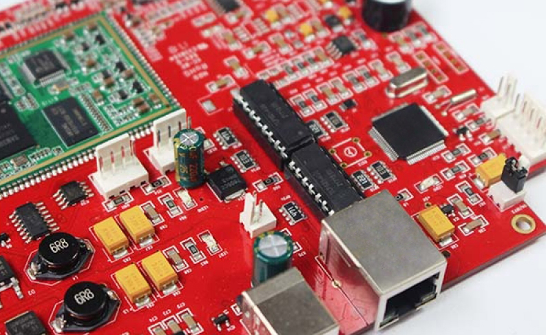
(Summary description)We know that PCBA processing is a rigorous and complicated process, and a little carelessness may cause a series of production problems. The circuit board is damaged at the slightest degree, and the safety accident may be easily caused by the serious incident, which threatens the personal safety of production personnel. Therefore, in the PCBA processing process, designers and operators must strictly understand the matters that need to be paid attention to. The following Sanjing will take everyone to understand:
1. In order to reduce the short circuit of the solder joints, all double-sided vias are prohibited from solder mask opening.
2. The upper tin position cannot have silk-screen printing.
3. There should be no copper foil and components within 5mm radius of the screw hole, except for grounding or according to the requirements of the structure drawing. The minimum distance between the copper foil and the board edge is 0.5mm, and the minimum distance between the component and the board edge is 5.0mm. The minimum distance between the pad and the edge of the board is 4.0mm.
4. The minimum gap between copper foils is 0.3mm for single-sided boards and...

Matters needing attention during PCBA processing
(Summary description)We know that PCBA processing is a rigorous and complicated process, and a little carelessness may cause a series of production problems. The circuit board is damaged at the slightest degree, and the safety accident may be easily caused by the serious incident, which threatens the personal safety of production personnel. Therefore, in the PCBA processing process, designers and operators must strictly understand the matters that need to be paid attention to. The following Sanjing will take everyone to understand:
1. In order to reduce the short circuit of the solder joints, all double-sided vias are prohibited from solder mask opening.
2. The upper tin position cannot have silk-screen printing.
3. There should be no copper foil and components within 5mm radius of the screw hole, except for grounding or according to the requirements of the structure drawing. The minimum distance between the copper foil and the board edge is 0.5mm, and the minimum distance between the component and the board edge is 5.0mm. The minimum distance between the pad and the edge of the board is 4.0mm.
4. The minimum gap between copper foils is 0.3mm for single-sided boards and...
- Categories:PCBA technical articles
- Author:SAJ
- Origin:
- Time of issue:2021-10-11
- Views:0
We know that PCBA processing is a rigorous and complicated process, and a little carelessness may cause a series of production problems. The circuit board is damaged at the slightest degree, and the safety accident may be easily caused by the serious incident, which threatens the personal safety of production personnel. Therefore, in the PCBA processing process, designers and operators must strictly understand the matters that need to be paid attention to. The following Sanjing will take everyone to understand:
1. In order to reduce the short circuit of the solder joints, all double-sided vias are prohibited from solder mask opening.
2. The upper tin position cannot have silk-screen printing.
3. There should be no copper foil and components within 5mm radius of the screw hole, except for grounding or according to the requirements of the structure drawing. The minimum distance between the copper foil and the board edge is 0.5mm, and the minimum distance between the component and the board edge is 5.0mm. The minimum distance between the pad and the edge of the board is 4.0mm.
4. The minimum gap between copper foils is 0.3mm for single-sided boards and 0.2mm for double-sided boards. When designing a double panel, pay attention to the components of the metal shell. The shell needs to be in contact with the PCB when plugging in. The top pad cannot be opened, and it must be sealed with silk screen oil or solder mask.
5. Jumpers are not allowed to be placed under the IC or under the components of potentiometers, motors and other large-volume metal casings.
6. The electrolytic capacitor is forbidden to touch the heating components. Such as transformers, thermistors, high-power resistors, radiators. The minimum distance between the radiator and the electrolytic capacitor is 10mm, and the distance between the remaining components and the radiator is 2mm.
7. Generally, the pad size (diameter) of through-hole mounting components is twice the diameter of the hole. The minimum size for double-sided boards is 1.5mm, and the minimum for single-sided boards is 2mm. The distance between the centers of the pads is less than 2.5mm, and the adjacent pads must be wrapped with silk-screen oil. The width of the silk-screen oil is 0.2mm. Large components (such as transformers, electrolytic capacitors with a diameter of 15mm or more, and high-current sockets) need to increase the pads.
8. For components that need to be soldered after soldering through a tin furnace, the solder pads must be driven away from the solder position, and the direction is opposite to the soldering direction. Mainly used for single-sided middle and post-welded pads to avoid blocking when passing the furnace.
9. In the large area PCB design, in order to prevent the PCB board from bending when passing through the soldering furnace, a gap of 5~10mm should be left in the middle of the PCB board to add a bend preventing bead when passing through the soldering furnace.
The above is about the precautions in the PCBA processing process, I hope it can be helpful to everyone!
Scan the QR code to read on your phone


Copyright©Sanjing Electronic Technology Co., Ltd. All Rights Reserved 粤ICP备09210657号
 400-1668-717

 Feedback