新闻资讯banner

PCB component layout and pad design
- Categories:SMT technology article
- Author:SAJ
- Origin:
- Time of issue:2021-12-21
- Views:0
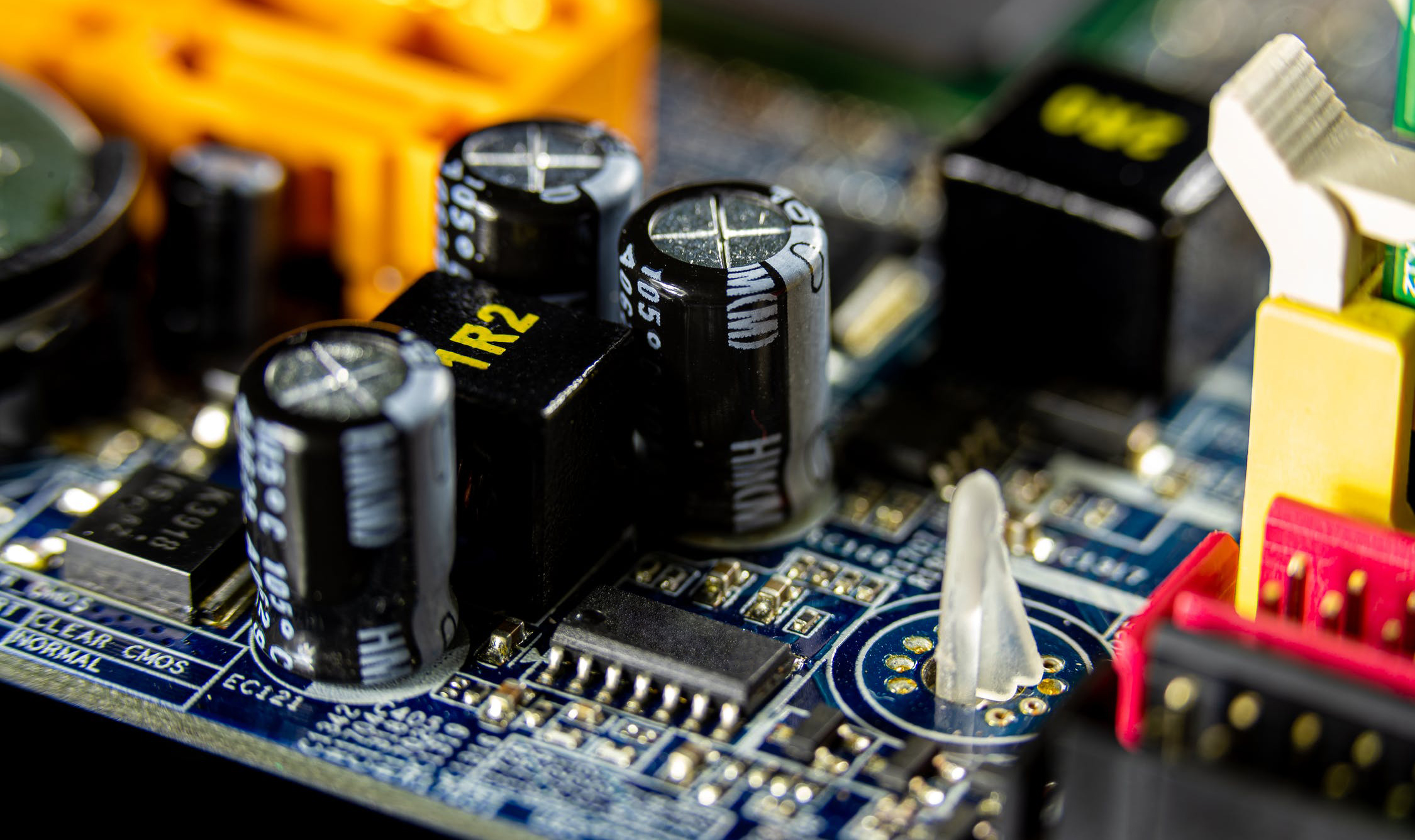
(Summary description)We know that the PCB will be designed before production. If the PCB design is unreasonable, it will affect the subsequent PCB production. Therefore, you need to pay attention to many issues when designing the PCB. The following Sanjing will let you know about the layout and welding of PCB components. Disk design.
(1) PCB component layout
① The components on the PCB should be evenly distributed, and the high-power components should be dispersed to avoid local overheating on the PCB when the circuit is working, which will affect the reliability of the solder joints.
②For double-sided mounting components, the larger components on both sides should be installed in a...

PCB component layout and pad design
(Summary description)We know that the PCB will be designed before production. If the PCB design is unreasonable, it will affect the subsequent PCB production. Therefore, you need to pay attention to many issues when designing the PCB. The following Sanjing will let you know about the layout and welding of PCB components. Disk design.
(1) PCB component layout
① The components on the PCB should be evenly distributed, and the high-power components should be dispersed to avoid local overheating on the PCB when the circuit is working, which will affect the reliability of the solder joints.
②For double-sided mounting components, the larger components on both sides should be installed in a...
- Categories:SMT technology article
- Author:SAJ
- Origin:
- Time of issue:2021-12-21
- Views:0
We know that the PCB will be designed before production. If the PCB design is unreasonable, it will affect the subsequent PCB production. Therefore, you need to pay attention to many issues when designing the PCB. The following Sanjing will let you know about the layout and welding of PCB components. Disk design.
(1) PCB component layout
① The components on the PCB should be evenly distributed, and the high-power components should be dispersed to avoid local overheating on the PCB when the circuit is working, which will affect the reliability of the solder joints.
②For double-sided mounting components, the larger components on both sides should be installed in a staggered position, otherwise the welding effect will be affected due to the increase of local heat capacity during the welding process.
③When the circuit board is placed on the conveyor belt of the reflow soldering furnace, the long axis of the components should be perpendicular to the direction of rotation of the equipment, which can prevent the components from drifting or "tombstones" on the board during the soldering process.
④The large and small SMT components on the wave soldering surface should not be lined up in a straight line, and the positions should be staggered to prevent false soldering and missing soldering due to the "shadow" effect of the solder wave crest during soldering.
⑤On the wave soldering surface, PLCC/QFP and other components with pins on four sides cannot be placed, and the long axis of the large SMT device installed on the wave soldering surface should be parallel to the direction of solder wave flow, which can reduce the electrode Solder bridging.
(2) PCB pad design
①The size of the pad should be determined according to the size of the component. The width of the pad is equal to or slightly larger than the width of the electrode of the component, and the welding effect is the best.
② For SMT components on the wave soldering surface, the pads of larger components (such as transistors, sockets, etc.) should be appropriately enlarged, so as to avoid empty soldering due to the "shadow effect" of the components.
③There should be no through holes on or near the pads of SMT components, otherwise the solder on the pads will flow away along the through holes after melting during the reflow process, resulting in false soldering, less tin, and possibly flowing to the board. Cause a short circuit on the other side.
④A single large pad should be avoided between two interconnected components, because the solder on the large pad will connect the two components to the middle. The correct way is to separate the pads of the two components. Use a thinner wire to connect between the two pads. If the wire is required to pass a larger current, several wires can be connected in parallel, and the wires are covered with green oil.
The above is about the layout of PCB components and pad design, I hope it can be helpful to everyone!
Scan the QR code to read on your phone


Copyright©Sanjing Electronic Technology Co., Ltd. All Rights Reserved 粤ICP备09210657号
 400-1668-717

 Feedback