新闻资讯banner

PCBA processing component layout requirements
- Categories:PCBA technical articles
- Author:SAJ
- Origin:
- Time of issue:2021-07-12
- Views:0
(Summary description)We know that in PCBA processing, the layout of components affects the quality of the SMT process, so the layout of PCBA processing components should meet the requirements of the SMT production process. This requires that when the components are laid out, the layout should be designed in accordance with the relevant process requirements. The correct layout design can minimize welding defects and ensure product quality. The following Sanjing will organize and introduce the layout requirements of PCBA processing components for everyone.
First of all, the layout requirements of components:
The components on the PCB should be arranged as regularly and evenly as possible. For components of the same type of...

PCBA processing component layout requirements
(Summary description)We know that in PCBA processing, the layout of components affects the quality of the SMT process, so the layout of PCBA processing components should meet the requirements of the SMT production process. This requires that when the components are laid out, the layout should be designed in accordance with the relevant process requirements. The correct layout design can minimize welding defects and ensure product quality. The following Sanjing will organize and introduce the layout requirements of PCBA processing components for everyone.
First of all, the layout requirements of components:
The components on the PCB should be arranged as regularly and evenly as possible. For components of the same type of...
- Categories:PCBA technical articles
- Author:SAJ
- Origin:
- Time of issue:2021-07-12
- Views:0
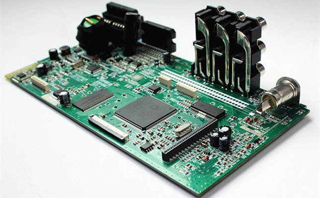
We know that in PCBA processing, the layout of components affects the quality of the SMT process, so the layout of PCBA processing components should meet the requirements of the SMT production process. This requires that when the components are laid out, the layout should be designed in accordance with the relevant process requirements. The correct layout design can minimize welding defects and ensure product quality. The following Sanjing will organize and introduce the layout requirements of PCBA processing components for everyone.
First of all, the layout requirements of components:
The components on the PCB should be arranged as regularly and evenly as possible. For components of the same type of package, the orientation, polarity, and spacing should be consistent as much as possible. The regular arrangement is convenient for inspection and helps to increase the patch/plug-in speed; the even distribution is good for the optimization of heat dissipation and welding process.
Secondly, the power components should be evenly placed on the edge of the PCB or on the ventilation position in the chassis to ensure good heat dissipation.
Third, leave a certain maintenance gap around the medium and large components (leave the size of the heater head of the SMD rework equipment capable of operation).
Fourth, do not place valuable components on the corners and edges of the PCB, or near the connectors, mounting holes, slots, cutting, gaps and corners of the jigsaw. These locations are high stress areas of the PCB, which are likely to cause soldering. Cracking of points and components.
Fifth, the layout of components on the wave soldering surface should meet the following requirements:
①Suitable for wave soldering, such as Chip type SMD components (SMD resistors, SMD capacitors, SMD inductors), SOT, SOP (lead center distance P≥1.27mm) with package size greater than or equal to 0603 (metric 1608) and above Etc., can not place fine-pitch devices.
②The height of the component should be less than the wave height of the wave soldering equipment.
③The extension direction of the component leads should be perpendicular to the PCB transfer direction during wave soldering, and two adjacent components must meet certain spacing requirements.
④The package of components on the soldering surface of wave soldering must be able to withstand temperatures above 260℃ and be fully sealed.
The above are some content about PCBA processing component layout requirements compiled by Sanjing for everyone, I hope it can be helpful to everyone!
Scan the QR code to read on your phone


Copyright©Sanjing Electronic Technology Co., Ltd. All Rights Reserved 粤ICP备09210657号
 400-1668-717

 Feedback