新闻资讯banner

Switch pcba manufacturer proofing process
- Categories:Switch pcba
- Author:
- Origin:
- Time of issue:2022-05-12
- Views:0
(Summary description)Before mass production of Switch pcbas, it is generally necessary for Switch pcba manufacturers to make samples first. The purpose is to make a small number of samples to test whether the quality of the products is qualified, and to a certain extent, avoid risks for future mass production. So, what is the proofing process for Switch pcba manufacturers?

Switch pcba manufacturer proofing process
(Summary description)Before mass production of Switch pcbas, it is generally necessary for Switch pcba manufacturers to make samples first. The purpose is to make a small number of samples to test whether the quality of the products is qualified, and to a certain extent, avoid risks for future mass production. So, what is the proofing process for Switch pcba manufacturers?
- Categories:Switch pcba
- Author:
- Origin:
- Time of issue:2022-05-12
- Views:0
Before mass production of Switch pcbas, it is generally necessary for Switch pcba manufacturers to make samples first. The purpose is to make a small number of samples to test whether the quality of the products is qualified, and to a certain extent, avoid risks for future mass production. So, what is the proofing process for Switch pcba manufacturers?
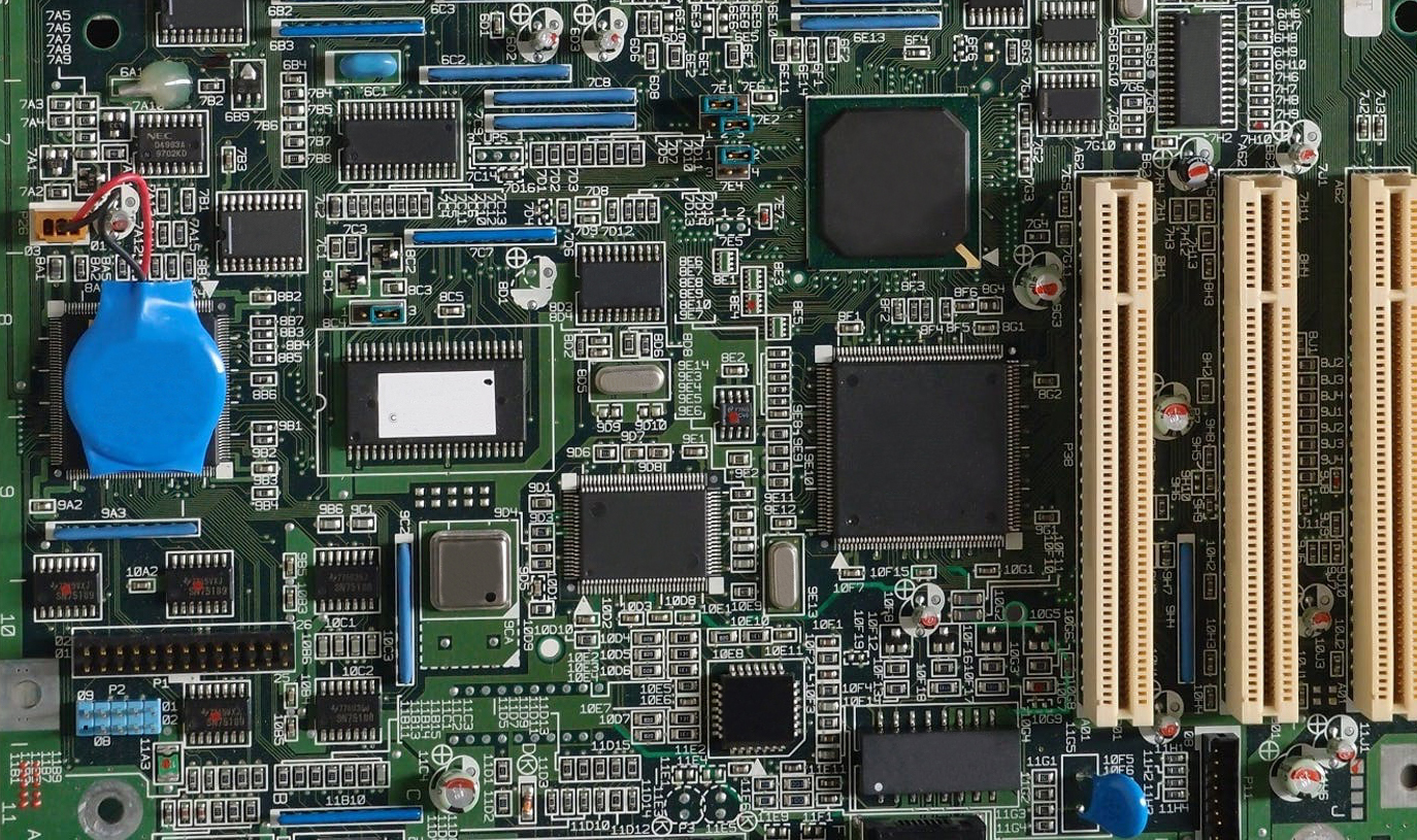
Step 1: Check the information
Before production, the Switch pcba manufacturer will check the board-making information provided by the customer, including the size of the board, process requirements and product quantity and other related data, and will only proceed to the next step of production after reaching an agreement with the customer.
The second step: open the material
The Switch pcba factory cuts out small pieces of production boards on the boards that meet the requirements according to the board materials given by the customers.
Step 3: Drilling
Drill the required hole diameter at the corresponding position of the Switch pcba.
The fourth step: sink copper
A thin layer of copper is chemically deposited on the insulating hole.
Step 5: Graphic Transfer
Transfer the image from the production film to the board.
Step 6: Graphic Plating
The Switch pcba factory electroplates a copper layer with the required thickness and a gold-nickel or tin layer with the required thickness on the exposed copper skin of the circuit pattern or the hole wall.
Step 7: Stripping
Remove the anti-plating coating layer with NaOH solution to expose the non-circuit copper layer.
Step 8: Etching
Remove the non-circuit parts with chemical reagent copper.
Step 9: Green Oil
Transfer the graphic of green oil film to the board, mainly to protect the circuit and prevent the tin on the circuit when welding parts.
Step 10: Characters
Recognizable characters are printed on the Switch pcba.
Step 11: Gold-plated fingers
A nickel/gold layer of the required thickness is plated on the plug fingers to make it more hard and wear-resistant.
Step 12: Forming
The Switch pcba factory will punch out the shape required by the customer with a die or a CNC gong machine.
Step 13: Test
It is not easy to find functional defects caused by open circuits, short circuits, etc. by visual inspection, and can be tested by a flying probe tester.
The above is the proofing process of the Switch pcba factory, I hope it will help you!
Scan the QR code to read on your phone
Relevant News


Copyright©Sanjing Electronic Technology Co., Ltd. All Rights Reserved 粤ICP备09210657号
 400-1668-717

 Feedback