新闻资讯banner

Switch pcba tells: the various aspects of the circuit board!
- Categories:Recommended news
- Author:
- Origin:
- Time of issue:2021-09-13
- Views:0
(Summary description)Signal layer: Mainly used to place components or wiring. Protel DXP usually contains 30 middle layers, namely Mid Layer1~Mid Layer30. The middle layer is used to arrange signal lines, and the top and bottom layers are used to place components or deposit copper.

Switch pcba
Signal layer: Mainly used to place components or wiring. Protel DXP usually contains 30 middle layers, namely Mid Layer1~Mid Layer30. The middle layer is used to arrange signal lines, and the top and bottom layers are used to place components or deposit copper.
Switch pcba tells: the various aspects of the circuit board!
(Summary description)Signal layer: Mainly used to place components or wiring. Protel DXP usually contains 30 middle layers, namely Mid Layer1~Mid Layer30. The middle layer is used to arrange signal lines, and the top and bottom layers are used to place components or deposit copper.
- Categories:Recommended news
- Author:
- Origin:
- Time of issue:2021-09-13
- Views:0
The circuit board includes many types of working layers, such as signal layer, protective layer, silk screen layer, internal layer, etc. Do you understand the role of various layers? Follow the Switch pcba editor for a simple understanding!
1. Signal layer: Mainly used to place components or wiring. Protel DXP usually contains 30 middle layers, namely Mid Layer1~Mid Layer30. The middle layer is used to arrange signal lines, and the top and bottom layers are used to place components or deposit copper.
2. Protective layer: It is mainly used to ensure that the parts of the circuit board that do not need to be tinned are not tinned, so as to ensure the reliability of the circuit board operation. Among them, Top Paste and Bottom Paste are the top solder mask and the bottom solder mask respectively; Top Solder and Bottom Solder are the solder paste protection layer and the bottom solder paste protection layer, respectively.
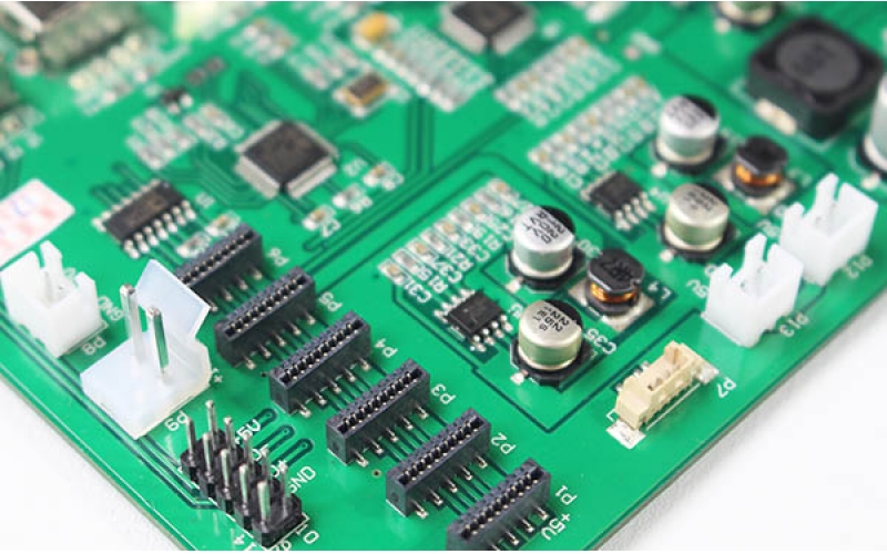
3. Silk screen layer: mainly used to print the serial number, production number, company name, etc. of the components on the circuit board.
4. Internal layer: Mainly used as a signal wiring layer. Protel DXP contains 16 internal layers.
5. Other layers: mainly include 4 types of layers.
Drilling azimuth layer: mainly used for the position of drilling holes on the printed circuit board. Prohibited wiring layer: mainly used to draw the electrical frame of the circuit board. Drilling drawing layer: mainly used to set the drilling shape. Multi-layer: Mainly used to set up multi-layers.
The above is the introduction of Switch pcba editor: a brief introduction to the level of knowledge about the circuit board.
Scan the QR code to read on your phone


Copyright©Sanjing Electronic Technology Co., Ltd. All Rights Reserved 粤ICP备09210657号
 400-1668-717

 Feedback