新闻资讯banner

The cheapest dimming control board analyzes the problems in PCB circuit design
- Categories:Cheapest Dimming control board
- Author:
- Origin:
- Time of issue:2022-03-19
- Views:0
(Summary description)The cheapest dimming control board pads (except surface mount pads) overlap: This also means that the holes overlap, and the drilling process will cause broken drill bits and hole damage due to multiple drilling in one place. Two holes in the multi-layer board overlap, for example, one hole is an isolation disk, and the other hole is a connection disk (flower pad), so that the negative is drawn as an isolation disk, resulting in scrap.

The cheapest dimming control board analyzes the problems in PCB circuit design
(Summary description)The cheapest dimming control board pads (except surface mount pads) overlap: This also means that the holes overlap, and the drilling process will cause broken drill bits and hole damage due to multiple drilling in one place. Two holes in the multi-layer board overlap, for example, one hole is an isolation disk, and the other hole is a connection disk (flower pad), so that the negative is drawn as an isolation disk, resulting in scrap.
- Categories:Cheapest Dimming control board
- Author:
- Origin:
- Time of issue:2022-03-19
- Views:0
1. The cheapest dimming control board pads (except surface mount pads) overlap: This also means that the holes overlap, and the drilling process will cause broken drill bits and hole damage due to multiple drilling in one place. Two holes in the multi-layer board overlap, for example, one hole is an isolation disk, and the other hole is a connection disk (flower pad), so that the negative is drawn as an isolation disk, resulting in scrap.
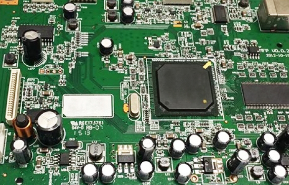
2. Single-sided pad aperture setting: Generally, single-sided pads are not drilled. If the drilling needs to be marked, the aperture should be designed to be zero. If the numerical value is designed, when the drilling data is generated, the coordinates of the hole will appear at that position, and finally the problem occurs.
3. Abuse of the graphics layer of the cheapest dimming control board: some useless connections are made on some graphics layers. It was originally a four-layer board but more than five layers of circuits were designed, which caused misunderstanding;
4. The characters are placed randomly: the characters cover the pad SMD solder tabs, which brings inconvenience to the on-off test of the printed board and the welding of components. If the characters are designed too small, it will make screen printing difficult, if they are too large, the characters will overlap each other and be difficult to distinguish.
5. The cheapest dimming control board uses filler blocks to draw pads: using filler blocks to draw pads can pass the DRC inspection when designing the circuit, but it is not possible for processing, so the similar pads cannot directly generate solder mask data. When the solder resist is applied, the fill block area will be covered by the solder resist, making it difficult to solder the device.
6. The cheapest dimming control board uses a combination of flower pads and wiring on the electrical ground: because the power supply is designed as a flower pad, the ground layer is opposite to the image on the actual printed board, and all the wires are isolated wires , the designer should be very clear about this.
Scan the QR code to read on your phone
Relevant News


Copyright©Sanjing Electronic Technology Co., Ltd. All Rights Reserved 粤ICP备09210657号
 400-1668-717

 Feedback