新闻资讯banner

The customized Switch pcba tells: Compatible design related knowledge of circuit board!
- Categories:Recommended news
- Author:
- Origin:
- Time of issue:2021-08-24
- Views:0
(Summary description)Choose a reasonable wire width. Because the impact interference generated by the transient current on the printed lines of the PCB circuit board is mainly caused by the inductance of the printed wires, the inductance of the printed wires should be minimized.

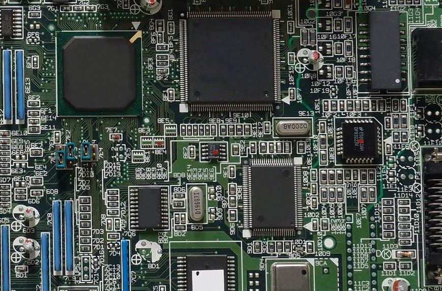
customized Switch pcba
Choose a reasonable wire width. Because the impact interference generated by the transient current on the printed lines of the PCB circuit board is mainly caused by the inductance of the printed wires, the inductance of the printed wires should be minimized.
The customized Switch pcba tells: Compatible design related knowledge of circuit board!
(Summary description)Choose a reasonable wire width. Because the impact interference generated by the transient current on the printed lines of the PCB circuit board is mainly caused by the inductance of the printed wires, the inductance of the printed wires should be minimized.
- Categories:Recommended news
- Author:
- Origin:
- Time of issue:2021-08-24
- Views:0
Electromagnetic compatibility refers to the ability of electronic equipment to work in a coordinated and effective manner in various electromagnetic environments. The purpose is to enable electronic equipment to suppress all kinds of external interference, so that the electronic equipment can work normally in a specific electromagnetic environment, and at the same time to reduce the electromagnetic interference of the electronic equipment itself to other electronic equipment. Let's follow the customized Switch pcba editor for a simple understanding!
1. Choose a reasonable wire width. Since the impact interference caused by the transient current on the printed lines of the PCB circuit board is mainly caused by the inductance of the printed wires, the inductance of the printed wires should be minimized.
2. Using the correct wiring strategy and equal wiring can reduce the wire inductance, but the mutual inductance and distributed capacitance between the wires increase. If the layout permits, it is recommended to use a grid-shaped wiring structure in the shape of a grid. The specific method is to wire one side of the printed board horizontally. , The other side is wired longitudinally, and then connected with metallized holes at the cross holes.
3. In order to suppress the crosstalk between the wires of the PCB circuit board, when designing the wiring, try to avoid long-distance equal wiring, and extend the distance between the wires as much as possible, and the signal wire and the ground wire and the power wire should not Cross. Setting a grounded printed line between some signal lines that are very sensitive to interference can effectively suppress crosstalk.
The above is the introduction of the customized Switch pcba editor: a brief introduction to the compatible design knowledge of the circuit board.
Scan the QR code to read on your phone


Copyright©Sanjing Electronic Technology Co., Ltd. All Rights Reserved 粤ICP备09210657号
 400-1668-717

 Feedback