新闻资讯banner

About the role of Switch pcba board vias and metal edging
- Categories:Switch pcba
- Author:
- Origin:
- Time of issue:2022-05-04
- Views:0
(Summary description)Circuit board, the full name of printed circuit board, is a bridge for signal communication between high-tech, among which there is an industrial control board that connects switches and machinery. A circle of vias and copper tapes are placed around, and even some RF boards will be metallized around the edges of the board.

About the role of Switch pcba board vias and metal edging
(Summary description)Circuit board, the full name of printed circuit board, is a bridge for signal communication between high-tech, among which there is an industrial control board that connects switches and machinery. A circle of vias and copper tapes are placed around, and even some RF boards will be metallized around the edges of the board.
- Categories:Switch pcba
- Author:
- Origin:
- Time of issue:2022-05-04
- Views:0
Circuit board, the full name of printed circuit board, is a bridge for signal communication between high-tech, among which there is an industrial control board that connects switches and machinery. A circle of vias and copper tapes are placed around, and even some RF boards will be metallized around the edges of the board.
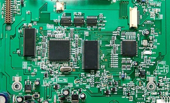
The edge radiation of the Switch pcba board is a relatively common source of electromagnetic radiation. Edge radiation occurs when unexpected currents reach the edges of the ground and power planes, with ground and power noise that manifests as: Insufficient power bypassing. The cylindrical radiated magnetic field generated by the inductive via radiates between the layers of the circuit board, eventually meeting at the edge of the circuit board. Stripline return currents that carry high frequency signals are too close to the edge of the board.
In order to prevent these situations, the Switch pcba board manufacturer recommends that a circle of ground vias be punched around the PCB with a 1/20 wavelength hole spacing to form a ground via shield to prevent TME waves from radiating to the outside. The Switch pcba board factory believes that for microwave circuit boards, the wavelength is further reduced, and due to the current PCB production process, the spacing between holes cannot be made very small.
The above is about the use of the circle of vias or metal edging around the Switch pcba board.
Scan the QR code to read on your phone


Copyright©Sanjing Electronic Technology Co., Ltd. All Rights Reserved 粤ICP备09210657号
 400-1668-717

 Feedback