新闻资讯banner

Causes and countermeasures of common defects in SMT welding
- Categories:FAQ
- Author:SAJ
- Origin:
- Time of issue:2021-08-30
- Views:0
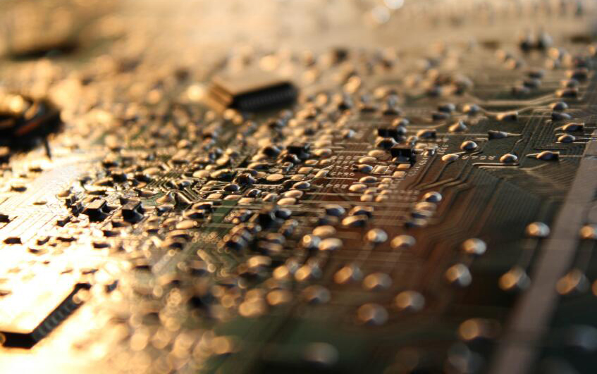
(Summary description)In the SMT production process, from the beginning of the mounting process to the end of the soldering process, the quality of the substrate is at zero defect is the biggest wish of SMT manufacturers. However, due to the many and complex SMT processes, there is no guarantee that each process will not go wrong. Therefore, in the SMT production process, we often encounter some welding defects. These defects are usually caused by various reasons. Let's take a look at Sanjing:
1. Bridging. Bridging often occurs on ICs with denser pins or between chip components with small spacing. This type of defect is a major defect in the inspection standard, which will seriously affect the electrical performance of the product and must be avoided. The main reason for this defect is the excessive amount of solder paste or the dislocation and edge collapse after the solder paste is printed.
2. Excessive solder paste. Excessive solder paste is caused by improper template thickness and opening size. Usually we...

Causes and countermeasures of common defects in SMT welding
(Summary description)In the SMT production process, from the beginning of the mounting process to the end of the soldering process, the quality of the substrate is at zero defect is the biggest wish of SMT manufacturers. However, due to the many and complex SMT processes, there is no guarantee that each process will not go wrong. Therefore, in the SMT production process, we often encounter some welding defects. These defects are usually caused by various reasons. Let's take a look at Sanjing:
1. Bridging. Bridging often occurs on ICs with denser pins or between chip components with small spacing. This type of defect is a major defect in the inspection standard, which will seriously affect the electrical performance of the product and must be avoided. The main reason for this defect is the excessive amount of solder paste or the dislocation and edge collapse after the solder paste is printed.
2. Excessive solder paste. Excessive solder paste is caused by improper template thickness and opening size. Usually we...
- Categories:FAQ
- Author:SAJ
- Origin:
- Time of issue:2021-08-30
- Views:0
In the SMT production process, from the beginning of the mounting process to the end of the soldering process, the quality of the substrate is at zero defect is the biggest wish of SMT manufacturers. However, due to the many and complex SMT processes, there is no guarantee that each process will not go wrong. Therefore, in the SMT production process, we often encounter some welding defects. These defects are usually caused by various reasons. Let's take a look at Sanjing:
1. Bridging. Bridging often occurs on ICs with denser pins or between chip components with small spacing. This type of defect is a major defect in the inspection standard, which will seriously affect the electrical performance of the product and must be avoided. The main reason for this defect is the excessive amount of solder paste or the dislocation and edge collapse after the solder paste is printed.
2. Excessive solder paste. Excessive solder paste is caused by improper template thickness and opening size. Usually we use 0.15mm thickness template. The opening size is determined by the smallest lead or chip component pitch.
3. Printing misalignment. When printing a printed board with a pin pitch or a chip pin pitch less than 0.65mm, optical positioning should be used and the reference point should be set at the diagonal of the printed board, otherwise it will cause printing misalignment due to positioning errors, resulting in bridging.
4. The solder paste collapses. There are three main types of welding edge collapse: printing edge collapse, edge collapse during mounting, and edge collapse during welding heating. ①Printing sag has a lot to do with the characteristics of solder paste, template, and printing parameter settings. For example, the viscosity of solder paste is low, the shape retention is not good, the wall of the template hole is rough and uneven, and the excessive scraper pressure has a greater impact on the solder paste. The impact force, the shape of the solder paste is destroyed, and the probability of collapse is greatly increased. Therefore, a higher viscosity solder paste can be selected, and a laser cutting board can be used to reduce the pressure of the squeegee.
②Sagging during mounting: When the placement machine is mounting SOP, QFP-type integrated circuits, the mounting pressure should be set appropriately, too much pressure will change the shape of the solder paste and cause sag. Therefore, it is necessary to adjust the placement pressure and set the lowering position of the placement nozzle including the thickness of the component itself.
③Sagging during soldering heating: When the printed board component is rapidly heating up, the solvent components in the solder paste will volatilize. If the volatilization speed is too fast, the solder particles will be squeezed out of the soldering area, thereby forming a sag during heating . Therefore, it is necessary to set an appropriate welding temperature curve (temperature/time) and prevent mechanical vibration of the conveyor belt.
5. Solder balls. Solder balls often appear on the sides of chip components or between fine-pitch pins. This situation is generally caused by the rapid heating during the soldering process to cause the solder splash. In addition to the above-mentioned printing misalignment and sagging, it is also related to the viscosity of the solder paste, the degree of solder paste oxidation, the particle size of the solder paste, and the flux. Activity and so on.
When the flux activity is low, solder balls are likely to be produced. In addition, if the printed board is not cleaned in place, there will be residual solder paste on the surface of the printed board and in the vias, and solder balls will be formed during soldering.
In addition to the more common soldering defects mentioned above, tombstones, pad size and thickness, placement offset, component weight, etc. are also more common in soldering. So, Sanjing will introduce you here today, I hope it can be helpful to everyone!
Scan the QR code to read on your phone


Copyright©Sanjing Electronic Technology Co., Ltd. All Rights Reserved 粤ICP备09210657号
 400-1668-717

 Feedback